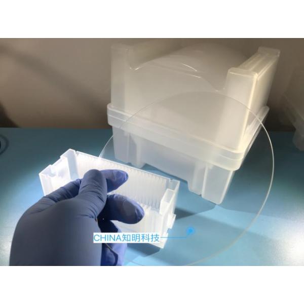
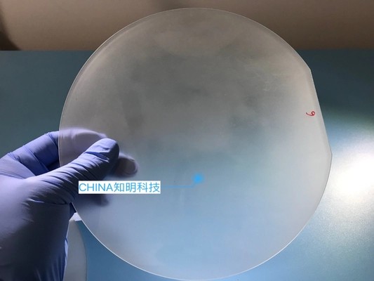
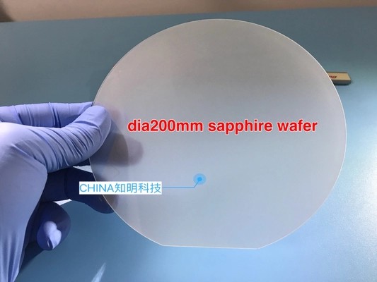
8" Sapphire Wafer 200mm Diameter (±0.2mm), 725µm Thickness, C-Plane SSP,DSP
This high-purity 8-inch (200mm) sapphire wafer features exceptional dimensional precision (±0.2mm diameter, 725µm thickness) and crystallographic orientation (C-plane), making it ideal for demanding optoelectronic and semiconductor applications. With 99.99% purity and superior mechanical/thermal stability, the wafer serves as an optimal substrate for LED, laser diode, and RF device fabrication. Its uniform surface finish and chemical inertness ensure reliability in harsh environments, while its large diameter supports cost-effective mass production.
Key Features of Sapphire Wafers
Sapphire Wafer's Precision Geometry:
- Diameter: 200mm ±0.2mm, ensuring compatibility with standard semiconductor tools.
- Thickness: 725µm ±25µm, optimized for mechanical strength and process stability.
Sapphire Wafer's Ultra-High Purity:
- >99.99% (4N) purity, minimizing impurities that affect optical/electrical performance.
Sapphire Wafer's Robust Material Properties:
- Hardness: 9 Mohs, scratch-resistant for handling durability.
- Thermal Stability: Melting point ~2,050°C, suitable for high-temperature processes.
- Optical Transparency: 85%+ in visible to near-IR spectra (350nm–4,500nm).
Sapphire Wafer's Surface Quality:
- Epitaxy-ready polish: Ra <0.3nm for defect-free thin-film deposition.
- Optional double-side polishing upon request.
Applications of Sapphire Wafers images
Sapphire wafer in Optoelectronics:
Substrate for blue/green/white LEDs (InGaN/GaN epitaxy).
Laser diodes (edge-emitting/VCSELs) in displays and communications.
Sapphire wafer in Power Electronics:
RF devices (5G/6G antennas, power amplifiers) due to low dielectric loss.
High-electron-mobility transistors (HEMTs) for electric vehicles.
Sapphire wafer in Industrial & Defense:
IR windows, missile domes (sapphire’s transparency to mid-IR).
Protective covers for sensors in corrosive/abrasive environments.
Sapphire wafer in Emerging Technologies:
Quantum computing (SPD crystal substrates).
Wearable device screens (scratch-resistant covers).
Specifications
| Parameter | Value |
| Diameter | 200mm ±0.2mm |
| Thickness | 725µm ±25µm |
| Orientation | C-plane (0001) ±0.2° |
| Purity | >99.99% (4N) |
| Surface Roughness (Ra) | <0.3nm (epi-ready) |
| TTV | ≤15um |
| WARP | ≤30um |
| BOW | -30~10um |
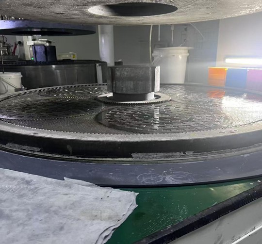
Factory Equipments


Product Tags:

|
|
Sapphire Wafer 8'' Dia 200mm±0.2mm Thickness 725Um C-Plane SSP,DSP hardness9.0 Images
|