DFB Epiwafer InP substrate MOCVD method 2 4 6 inch Operating wavelength: 1.3 µm, 1.55 µm
DFB Epiwafer InP substrate's Brief
DFB (Distributed Feedback) Epiwafers on Indium Phosphide (InP) substrates are key components used in fabricating high-performance DFB laser diodes. These lasers are critical for optical communication and sensing applications due to their ability to produce single-mode, narrow-linewidth light with stable wavelength emission, typically in the 1.3 µm and 1.55 µm ranges.
The InP substrate provides excellent lattice matching for epitaxial layers such as InGaAsP, which are grown to form the active region, cladding layers, and grating structures that define the DFB laser's functionality. The integrated grating within the structure ensures precise feedback and wavelength control, making it suitable for long-distance fiber-optic communication and WDM (Wavelength Division Multiplexing) systems.
Key applications include high-speed optical transceivers, data center interconnects, gas sensing, and optical coherence tomography (OCT). The InP-based DFB epiwafer's combination of high-speed performance, narrow spectral linewidth, and wavelength stability makes it indispensable in modern telecommunication networks and advanced sensing technologies.
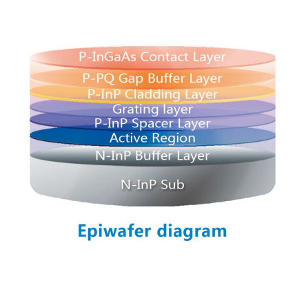
DFB Epiwafer InP substrate's structure
DFB Epiwafer InP substrate's datasheet(ZMSH DFB inp epiwafer.pdf)

DFB Epiwafer InP substrate's properties
Substrate Material:
- Indium Phosphide (InP): InP provides an excellent lattice match for epitaxial layers like InGaAsP, reducing defects and dislocations during the epitaxial growth process. This leads to high-quality layers essential for efficient laser performance.
Bandgap:
- Direct Bandgap: InP has a direct bandgap of 1.344 eV, making it highly suitable for optoelectronic applications, particularly for emission in the infrared spectrum, around the 1.3 µm and 1.55 µm wavelengths, which are optimal for optical communication.
Lattice Matching:
- InP allows the growth of high-quality epitaxial layers, especially InGaAsP, with minimal strain, ensuring stable and reliable device operation.
Epitaxial Layers:
- Active Layer: Usually composed of InGaAsP, this layer defines the emission wavelength and supports the generation of photons through radiative recombination.
- Grating Structure: The integrated grating within the epitaxial structure provides the feedback needed for single-mode emission, essential for wavelength precision in DFB lasers.
- Cladding Layers: Surrounding the active region, these layers confine the light and direct it towards the output facet, ensuring efficient optical confinement.
Operating Wavelength:
- 1.3 µm and 1.55 µm: These wavelengths are ideal for fiber-optic communication because of their low loss in optical fibers, making DFB lasers crucial for long-distance and high-speed data transmission.
Narrow Linewidth and Single-Mode Operation:
- DFB lasers provide a narrow spectral linewidth and operate in single longitudinal mode, which is critical for minimizing signal interference and maximizing data integrity in dense Wavelength Division Multiplexing (WDM) systems.
Temperature Stability:
- InP-based DFB lasers offer excellent temperature stability, which is essential for maintaining consistent wavelength output and minimizing performance degradation over varying operational temperatures.
Low Threshold Current:
- DFB lasers on InP substrates exhibit low threshold currents, leading to energy-efficient operation, which is beneficial for both performance and power consumption, particularly in data centers and telecommunication networks.
High-Speed Modulation Capability:
- InP-based DFB lasers support high-speed modulation, making them ideal for use in optical transceivers and communication systems that require rapid data transfer.
The key properties of DFB Epiwafers on InP substrates, such as their excellent lattice matching, single-mode operation, narrow linewidth, high-speed performance, and temperature stability, make them indispensable for optical communication, sensing, and advanced photonic applications.
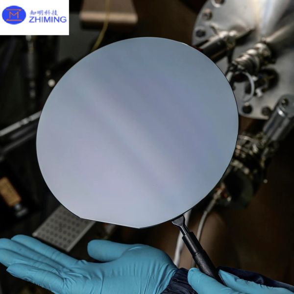
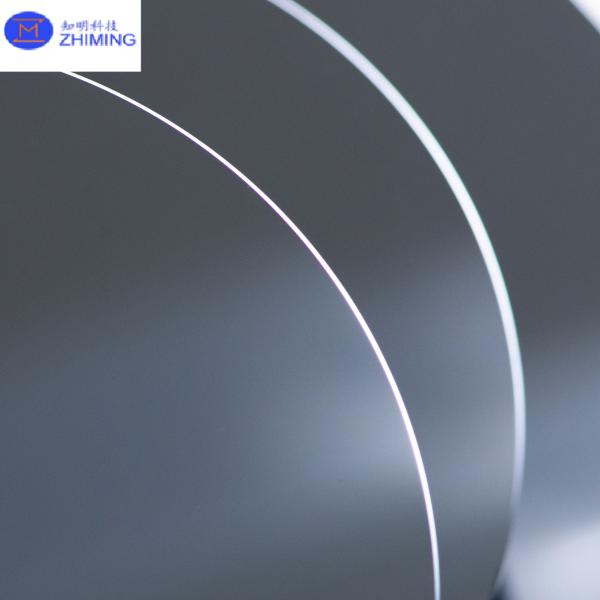
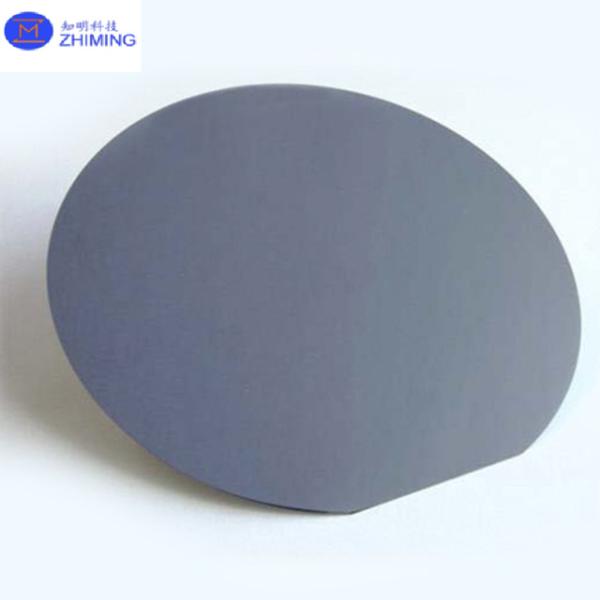
DFB Epiwafer InP substrate's real photos

DFB Epiwafer InP substrate's application
1. Optical Communication
- Long-Distance Fiber Optic Networks: DFB lasers are critical for long-distance optical communication, particularly in the 1.3 µm and 1.55 µm wavelength ranges, where signal loss in optical fibers is minimized. These lasers are essential for high-speed data transmission over long distances.
- WDM (Wavelength Division Multiplexing) Systems: DFB lasers are used in WDM systems to transmit multiple data channels over a single fiber by assigning each channel a specific wavelength. Their wavelength precision and stability are vital for avoiding interference between channels.
2. Data Center Interconnects
- High-Speed Data Transmission: DFB lasers are employed in data centers to connect servers and networking equipment, providing high-speed optical links that handle large amounts of data with minimal signal loss and interference.
3. Gas Sensing and Environmental Monitoring
- Gas Detection: DFB lasers are used in gas sensing applications to detect specific gases, such as CO2 and CH4, by tuning the laser to match the absorption lines of these gases. This is critical for industrial safety, environmental monitoring, and emissions control.
- Laser Absorption Spectroscopy: In environmental monitoring, DFB lasers enable precise measurement of gas concentrations, leveraging their narrow linewidth and tunable wavelengths for high-resolution detection.
4. Optical Coherence Tomography (OCT)
- Medical Diagnostics: DFB lasers are utilized in OCT systems for non-invasive medical imaging, such as retinal scans in ophthalmology and tissue imaging in dermatology. The stable wavelength and narrow spectral linewidth enhance the resolution and clarity of the images.
5. LIDAR (Light Detection and Ranging)
- Autonomous Vehicles and 3D Mapping: DFB lasers are integral to LIDAR systems, which are used for distance measurement and object detection in autonomous vehicles, drones, and 3D mapping applications. The laser's precision and stability improve the accuracy of LIDAR systems in determining distances and identifying objects.
6. Satellite and Space Communication
- High-Frequency Communication: DFB lasers are used in satellite communication systems, where long-distance, high-frequency data transmission is required. The ability of DFB lasers to maintain a stable wavelength under varying environmental conditions is crucial for space communication.
Key worlds: InP substrate DFB epiwafer
Product Tags:

|
|
DFB Epiwafer InP Substrate MOCVD Method 2 4 6 Inch Operating Wavelength 1.3 Μm, 1.55 Μm Images
|